


Discount Price Te Sputtering Target - Niv Sputtering Target High Purity Thin Film Pvd Coating Custom Made – Rich
Discount Price Te Sputtering Target - Niv Sputtering Target High Purity Thin Film Pvd Coating Custom Made – Rich Detail:
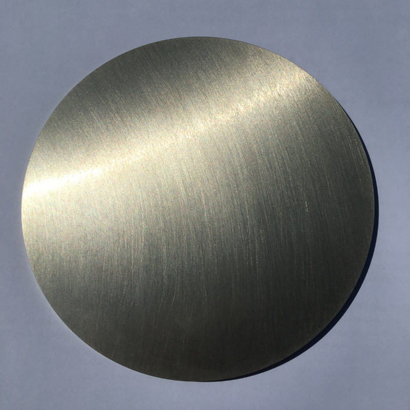
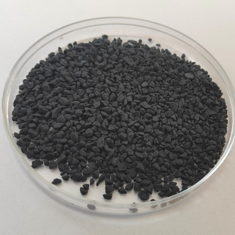
Nickel Vanadium Sputtering Target Description
Gold is often applicated in the deposition of integrated circuit layer, but AuSi low-melting compound is often formed if Gold is combined with Silicon, which would cause the looseness between different layers. Pure Nickel is a good choice for Adhesive layer, while a Barrier layer is also required between the Nickel and Gold layer to prevent proliferation. Vanadium could perfectly satisfy this requirement with high melting point and capacity of standing high ampere density. Therefore Nickel, Vanadium and Gold are three materials usually applicated in integrated circuit industry. Nickel Vanadium Sputtering Target is manufactured by adding Vanadium into molten Nickel. With low ferromagnetism, it is a good choice for the magnetron sputtering of electronic products, which could produce Nickel layer and Vanadium layer in one time.
Ni-7V wt% Impurity Content
|
Purity |
Main Component(wt%) |
Impurity Chemicals(≤ppm) |
Impurity In total(≤ppm) |
||||||
|
V |
Fe |
Al |
Si |
C |
N |
O |
S |
||
|
99.99 |
7±0.5 |
20 |
30 |
20 |
100 |
30 |
100 |
20 |
100 |
|
99.95 |
7±0.5 |
200 |
200 |
200 |
100 |
100 |
200 |
50 |
500 |
|
99.9 |
7±0.5 |
300 |
300 |
300 |
100 |
100 |
200 |
50 |
500 |
Nickel Vanadium Sputtering Target Packaging
Our Nickel Vanadium sputter target is clearly tagged and labeled externally to ensure efficient identification and quality control. Great care is taken to avoid any damage which might be caused during storage or transportation.
Get Contact
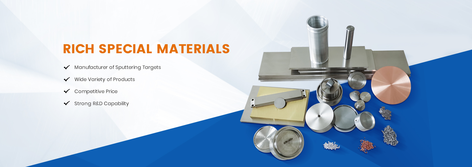
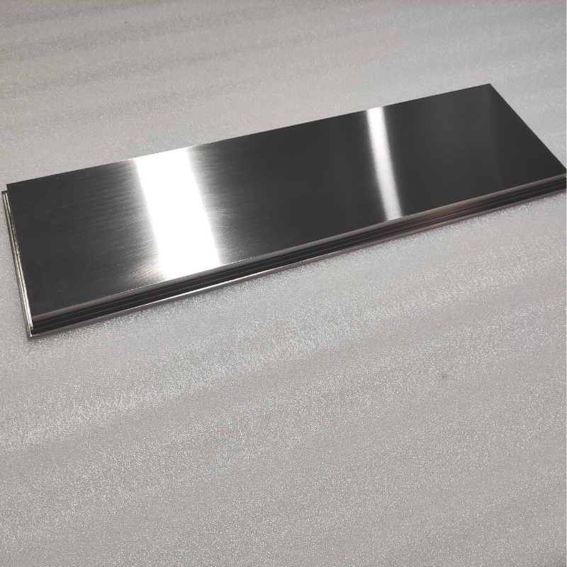
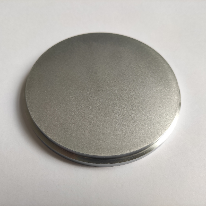
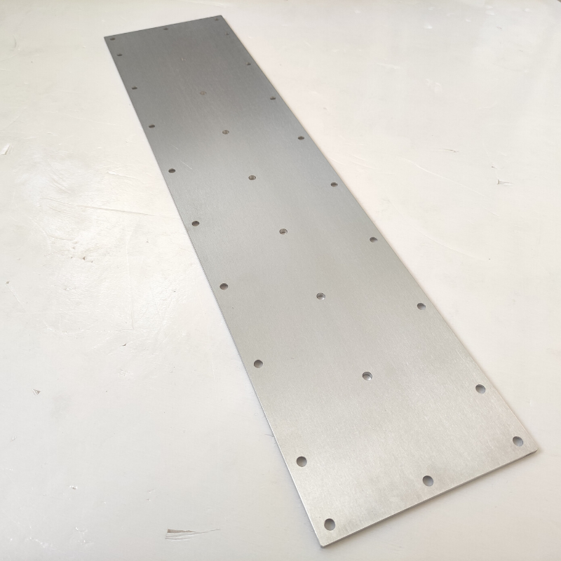
RSM’s Nickel Vanadium sputtering targets are of ultra-high purity and uniform. They are available in various forms, purities, sizes, and prices. We specialize in producing high purity thin film coating materials with excellent performance as well as the highest possible density and smallest possible average grain sizes for use in mold coating、decoration、automobile parts、low-E glass、semi-conductor integrated circuit、thin film resistance、graphic display、aerospace、 magnetic recording、touch screen、thin film solar battery and other physical vapor deposition (PVD) applications. Please send us an inquiry for current pricing on sputtering targets and other deposition materials not listed.
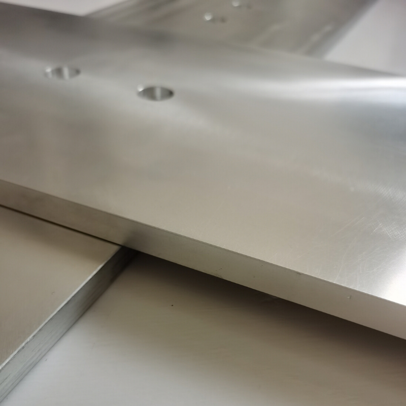
Product detail pictures:
Related Product Guide:
We take "customer-friendly, quality-oriented, integrative, innovative" as objectives. "Truth and honesty" is our administration ideal for Discount Price Te Sputtering Target - Niv Sputtering Target High Purity Thin Film Pvd Coating Custom Made – Rich , The product will supply to all over the world, such as: Iran, Surabaya, Curacao, With a wide range, good quality, reasonable prices and stylish designs, our products are extensively used in this field and other industries. We welcome new and old customers from all walks of life to contact us for future business relationships and achieving mutual success! We welcome customers, business associations and friends from all parts of the world to contact us and seek cooperation for mutual benefits.
Cooperate with you every time is very successful, very happy. Hope that we can have more cooperation!
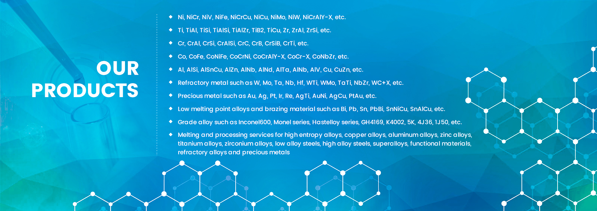
Products categories
-
Big Discount Tb Sputtering Target - High purit...
-
professional factory for Nickel Pieces - Niobi...
-
Manufactur standard Nipt Sputtering Target - C...
-
Chinese Professional Sputtering Target Sheet -...
-
Fast delivery Aluminum Niobium Sputtering Targe...
-
Reliable Supplier Tellurium Te Sputtering Targe...