
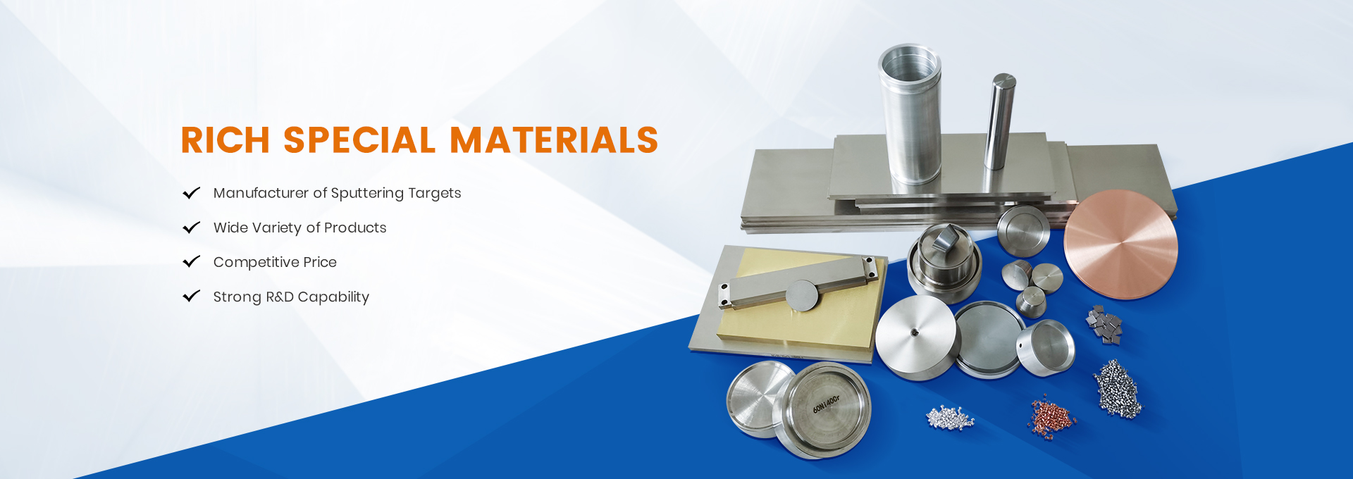
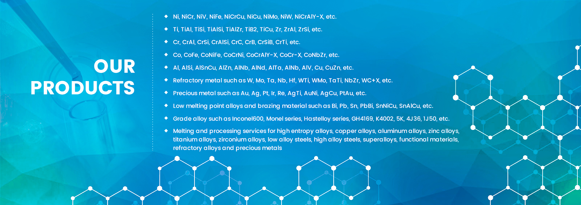


Rich Special Material Co., Ltd. can produce high-purity aluminum sputtering targets, copper sputtering targets, tantalum sputtering targets, titanium sputtering targets, etc. for the semiconductor industry.
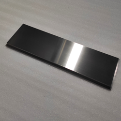
Semiconductor chips have high technical requirements and high prices for sputtering targets. Their requirements for the purity and technology of sputtering targets are higher than those of flat panel displays, solar cells and other applications. Semiconductor chips set extremely strict standards on the purity and internal microstructure of sputtering targets. If the impurity content of the sputtering target is too high, the film formed cannot meet the required electrical properties. In the sputtering process, it is easy to form particles on the wafer, resulting in short circuit or circuit damage, which seriously affects the performance of the film. Generally speaking, the highest purity sputtering target is required for chip manufacturing, which is usually 99.9995% (5N5) or higher.
Sputtering targets are used for the fabrication of barrier layers and packaging metal wiring layers. In the wafer manufacturing process, the target is mainly used to make the conductive layer, barrier layer and metal grid of the wafer. In the process of chip packaging, the sputtering target is used to generate metal layers, wiring layers and other metal materials under the bumps. Although the amount of target materials used in wafer manufacturing and chip packaging is small, according to SEMI statistics, the cost of target materials in wafer manufacturing and packaging process accounts for about 3%. However, the quality of the sputtering target directly affects the uniformity and performance of the conductive layer and barrier layer, thereby affecting the transmission speed and stability of the chip. Therefore, the sputtering target is one of the core raw materials for semiconductor production
Post time: Nov-16-2022