
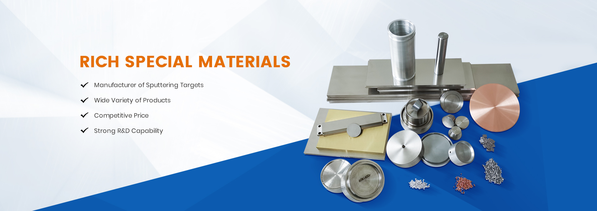


1. What is Sputtering? The Core Concept in One Sentence
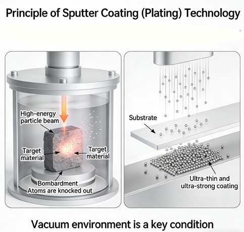
Sputtering (also known as sputter coating) is an advanced technology that, within a vacuum environment, uses high-energy particles to “bombard” a solid material, “knocking” its atoms out one by one, and then allowing these atoms to fall like a fine rain onto the surface of another object, forming an ultra-thin, ultra-strong coating.
Simply put, it’s like ”spray painting at the atomic level”—but instead of a brush, it uses microscopic “energy projectiles” to precisely “transport” atoms from one material to another.
2. Why Do We Need Sputtering? The Limitations of Traditional Methods
To understand the underlying logic of sputtering, we must first understand the problems it solves:
Traditional coating methods (like evaporation) are like “drying clothes in the sun”—relying on heat to evaporate the material, which then naturally deposits. But this method has three major flaws:
1.Heat Sensitivity: Many precision components (like chips, plastic lenses) cannot withstand high temperatures.
2.Non-Uniformity: Similar to drying clothes in the sun, there can be significant differences between shaded and exposed areas.
3.Poor Adhesion: The coating can easily flake off with a light scratch.
Sputtering technology is precisely the “intelligent solution” born to address these pain points.
Step 4: The Wisdom of “Building a New City”—Atomic Deposition and Film Formation
The “knocked-out” target atoms travel through the vacuum and, upon reaching the substrate surface:
1.Adsorption: Atoms temporarily “stick” to the surface.
2.Migration: Using their remaining energy, they “search for a spot” on the surface.
3.Nucleation and Growth: Atoms meet, bond, and gradually cover the entire surface.
4.Film Formation: Layer upon layer of atoms stack up, eventually forming a functional coating only nanometers thick.
The Core Logic of the Entire Process: Converting electrical energy → into plasma potential energy → into ion kinetic energy → into atomic sputtering energy → finally solidifying into the binding energy of the thin film.
4. The Unique Advantages of Sputtering: Why It’s Irreplaceable?
| Advantage | Specific Manifestation | Practical Significance |
|---|---|---|
| Low-Temperature Process | Substrate temperature can be below 100°C | Allows coating of plastics, paper, precision chips. |
| Superb Adhesion | Atoms are “embedded,” not just “stuck on” | Coating is extremely difficult to peel off, long service life. |
| Extreme Uniformity | Atomic-level precision control | Perfect coverage even on complex curved surfaces. |
| Material Versatility | Can sputter metals, ceramics, alloys, etc. | Almost no material limitations. |
| Eco-Friendly & Safe | Physical process, no toxic chemicals | Aligns with green manufacturing trends. |
5. Sputtering is All Around You: Ubiquitous Applications
1. Electronics & Digital
1.Smartphone/Tablet Screens: Transparent ITO conductive film (core of touch functionality).
2.Chip Manufacturing: Nanoscale metal interconnects and insulating layers.
3.Hard Disk Drives: Ultrathin magnetic recording layers.
2. Optics & Displays
Eyeglass Lenses: Multi-layer coatings for anti-reflection and scratch resistance.
Camera Lenses: Enhance light transmission, eliminate glare.
Architectural Glass: Low-E (low-emissivity) insulating coatings.
3. Daily Life & Industry
Tool Coatings: Increase hardness, corrosion resistance (e.g., TiN gold-colored coating).
Watches & Jewelry: High-end finishes like rose gold, black.
Packaging Materials: Oxygen/moisture barrier layers for food packaging.
6. The Evolution of Sputtering Tech: From Basic to Cutting-Edge
1.DC Sputtering: The most basic version, can only coat conductive materials.
2.RF (Radio Frequency) Sputtering: A breakthrough! Can coat insulating materials (glass, ceramics).
3.Magnetron Sputtering: A revolutionary advance! Uses magnetic fields to confine electrons, increasing efficiency tenfold.
4.Reactive Sputtering: Combines sputtering with chemical reactions to directly synthesize compound films.
The underlying logic of sputtering is using physical “destruction” to achieve material “reconstruction.” It doesn’t use heat or melting. Instead, through precisely controlled “microscopic collisions,” it “transports” atoms from one material to the surface of another, achieving a functional reconstruction at the atomic level.
The brilliance of this technology lies in this: it transforms what seems like a “violent” ion bombardment into an extremely precise manufacturing process. From a smartphone to the mirror of a space telescope, sputtering technology is quietly shaping the modern world we see, use, and rely on.
With the development of frontiers like flexible electronics, metaverse displays, and quantum computing, this technology capable of “painting” at the atomic scale is destined to play an even more critical role—because what it achieves is not simply a “cover,” but a functional re-engineering of material surfaces.
Post time: Jan-29-2026