


Behind the brilliant screens of smartphones, the billions of transistors in computer chips, the thin heat-insulating films on car windows, and even the protective coatings on spacecraft surfaces lies a crucial foundational material—the sputtering target. Although not directly visible in the final product, it is a core consumable material for manufacturing these high-tech devices, hailed as the ”invisible cornerstone” or ”sustenance” of modern electronics and advanced manufacturing.
1. What is a Sputtering Target?
Simply put, a sputtering target is a material that, within an ultra-high vacuum environment, is bombarded by high-speed ion beams (a process called “sputtering”). This causes its atoms or molecules to be ejected and steadily deposited onto a substrate surface (such as a silicon wafer, glass, or plastic), forming a thin, precise film.
You can think of it as:
An “Ink Cartridge”: The target is the source of the “ink,” and the substrate is the “paper” to be printed on.
“Microscopic Cannonball Bombardment”: Energetic ions act like cannonballs, “knocking off” atoms one by one from the target’s surface. These atoms fly toward the substrate and firmly adhere, building up a film layer by layer like laying bricks.
2. Core Technical Principle: Physical Vapor Deposition (PVD) – Sputtering Coating
Sputtering is a primary method of Physical Vapor Deposition (PVD). The basic process is as follows:
1.Vacuum Environment: The target and the substrates to be coated are placed inside a highly evacuated coating chamber.
2.Plasma Generation: An inert gas (usually argon) is introduced, and a high voltage is applied, ionizing the argon gas to form a plasma filled with positive ions and electrons.
3.Bombarding the Target: Driven by the electric field, positively charged argon ions accelerate and strike the target (cathode) at high speed.
4.Atom Sputtering: Atoms or molecules on the target surface gain kinetic energy, break free from the surface, and travel towards the substrate as atomic vapor.
5.Thin Film Formation: The dispersed target atoms deposit and condense on the substrate surface, gradually forming a dense, uniform, and firmly bonded thin film.
By precisely controlling process parameters, ultra-pure films with thicknesses ranging from nanometers to micrometers and possessing specific functionalities (conductive, insulating, optical, wear-resistant, etc.) can be fabricated.
3. Classification of Sputtering Targets
Targets come in many varieties and can be classified from different perspectives:
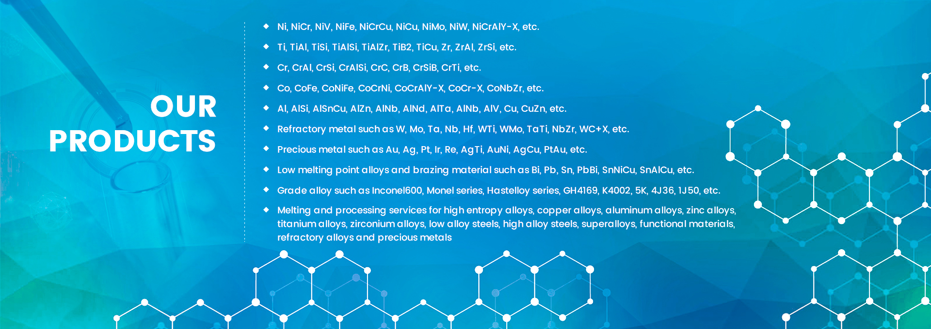
1. By Chemical Composition (The most fundamental classification):
Metallic Targets: Such as aluminum, copper, titanium, tantalum, nickel, chromium. Primarily used for conductive layers, electrodes, barrier layers, decorative coatings, etc.
Example Application: Copper interconnects inside chips, the metallic luster on smartphone casings.
Alloy Targets: Such as nickel-chromium alloys, cobalt-based alloys, titanium-aluminum alloys. Used to achieve special properties not possible with single metals.
Example Application: Thin-film resistors, magnetic storage layers.
Ceramic (Compound) Targets: Such as Indium Tin Oxide (ITO), silicon oxide, titanium nitride, aluminum nitride.
Example Application: ITO targets are core to the transparent conductive films in touchscreens; titanium nitride is used for golden decorative coatings and super-hard wear-resistant coatings.
Semiconductor Targets: Such as silicon, germanium, gallium arsenide. Mainly used in integrated circuit manufacturing.
2. By Shape:
Planar Targets: The most common, rectangular or circular in shape.
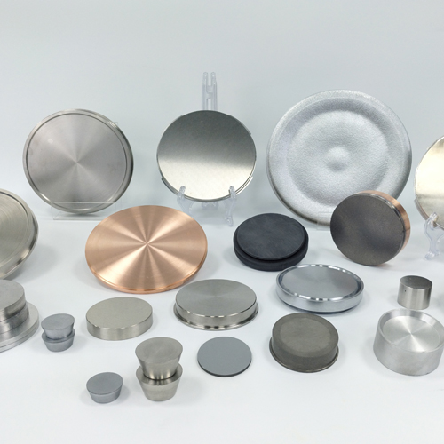
Rotary Targets (Rotatable Targets): Cylindrical, capable of rotating around an axis. Higher material utilization (can exceed 80%), excellent film uniformity, and longer lifespan. Have become the mainstream choice for large-area coating (e.g., architectural glass, photovoltaic cells).

3. By Application Field:
Semiconductor Chip Targets: Require the highest purity (typically ≥99.9995% or 5N5), representing the highest technical barrier. Involve high-purity metals and their alloys like Al, Cu, Ta, Ti, Co.
Flat Panel Display (FPD) Targets: The largest market segment. Primarily ITO targets, along with metallic targets like molybdenum, copper, and aluminum.
Photovoltaic (PV) Cell Targets: Mainly used for electrodes and functional layers in thin-film solar cells, e.g., aluminum, copper, molybdenum, ITO.
Information Storage Targets: Used for magnetic recording media in hard disks, optical discs, e.g., cobalt-chromium-platinum alloys.
Optical Coating Targets: For anti-reflection, reflective films on lenses, glasses, automotive glass, e.g., silicon dioxide, titanium dioxide, tantalum pentoxide.
Tool Modification/Decorative Coating Targets: Such as titanium nitride (golden), chromium nitride (silvery), titanium carbide, used to enhance tool hardness, wear resistance, and for decoration.
4. Why are Sputtering Targets So Important and Challenging?
1.High Purity Requirements: Especially in semiconductors, trace impurities can cause chip circuit failure or performance degradation. Producing ultra-high purity metals (e.g., >6N, 99.9999%) and maintaining that purity is a core technology.
2.High Density and Uniformity: Targets must be highly dense internally, with uniform composition (low segregation), fine and uniform grain structure. Any micro-porosity or compositional non-uniformity can cause defects in the film.
3.High-Precision Processing and Bonding: Targets need to be tightly bonded (via welding/soldering) to a backing plate (usually copper) to ensure good thermal and electrical conductivity. Bonding quality directly affects target lifespan and performance, with yield rate being a key cost factor.
4.High Industry Certification Barriers: Downstream customer (e.g., chip makers, panel fabs) certification cycles are extremely long (2-3 years). Once integrated into the supply chain, stable partnerships form, making it difficult for new entrants to break in.
5. Industry Status and Trends
1.Industry Chain: Upstream involves high-purity metal refining; midstream involves target manufacturing and bonding; downstream includes applications in semiconductors, displays, photovoltaics, etc.
2.Technology Trends:
Large-Sizing: To meet the demands of G10.5/11 Gen LCD panels and larger silicon wafers (300mm and above).
Higher Purity and Composition Complexity: To meet the demands of advanced process nodes (e.g., 3nm, 2nm) for new materials like cobalt, ruthenium.
Popularization of Rotary Targets: To improve material utilization, coating uniformity, and reduce production costs.
Recycling: Recycling and regeneration technology for spent targets is a crucial link in cost reduction.
Conclusion
Sputtering targets are a critical link connecting basic raw materials to cutting-edge end products. Though “invisible,” they directly determine the performance of integrated circuits, the clarity of display panels, the conversion efficiency of solar cells, and the reliability of various high-end components. With the rapid development of industries like 5G, AI, IoT, and new energy, the demand for high-performance, specialized sputtering targets will continue to grow, and their strategic importance will become even more prominent. Mastering the core technology of targets is a vital cornerstone for achieving supply chain autonomy and driving manufacturing upgrades.
Post time: Dec-19-2025