
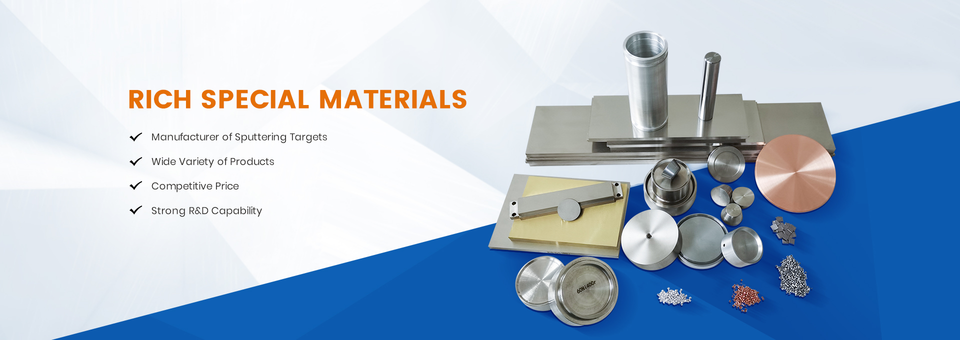
In the semiconductor industry and electronic thin film preparation, the performance of sputtering targets directly determines the quality of deposited films, and the backing plate bonding technology behind the target is an indispensable key link in this process.
During physical vapor deposition (PVD), sputtering targets endure continuous bombardment by high-energy ions, operating in harsh environments characterized by high voltage and high vacuum. Since most target materials inherently lack sufficient strength, and require effective heat conduction and electrical conduction, backplate bonding technology has emerged to meet these needs.
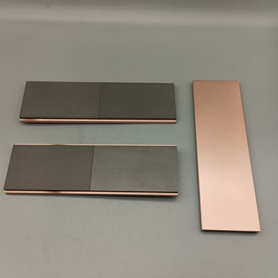
The backplate not only supports the target but also must possess good electrical and thermal conductivity. Common backplate materials are copper or copper alloys.
01 Core Functions of the Backplate: Why is Bonding Indispensable?
In the semiconductor chip coating process, the target assembly operates in an extremely harsh environment: temperatures can reach 300°C to 600°C, with one side intensely cooled by circulating water and the other side in a high vacuum of up to 10⁻⁹ Pa.
Such working conditions place extremely high demands on the target assembly, making the role of the backplate crucially important.
Support and Fixation are the primary functions of the backplate. Most high-purity metal targets (such as scandium targets) lack sufficient mechanical strength themselves and require a backplate as a supporting structure to be fixed within the sputtering machine.
Without the support of a backplate, the target is prone to deformation or cracking under high-speed ion bombardment.
Thermal Management is another critical function of the backplate. During the sputtering process, ion bombardment generates significant heat. The backplate acts as a thermal conductor, rapidly transferring this heat to the cooling system to prevent target overheating.
One side of the target assembly is strongly cooled by circulating water, for which the good thermal conductivity of the backplate is essential.
Regarding Electrical Conduction, the backplate serves as part of the electrode, providing the necessary current path for the sputtering process. The backplate must have good electrical conductivity to ensure the stability of the sputtering process.
The backplate also helps increase target utilization. Through rational structural design, it ensures uniform sputtering of the target material, reducing material waste, which is particularly important for expensive target materials like high-purity scandium.
02 Bonding Methods: Analysis of Four Mainstream Technologies
Brazing
Brazing uses a metal or alloy filler material (solder) with a melting point lower than the base materials. The melted solder fills the joint gap upon heating, creating the connection.
Indium brazing is one widely used method, especially in bonding high-purity metal scandium targets.
Advantages of brazing include: Mature technology, suitable for large-area welding, and relatively low operating temperatures.
However, brazing also has obvious disadvantages: the bond strength is typically below 70 MPa, and the solder used (such as pure indium) can be expensive, increasing the bonding cost.
Conductive Adhesive Bonding
Conductive adhesive bonding uses polymer materials filled with metal particles to achieve connection, mainly including Isotropic Conductive Adhesives (ECA) and Anisotropic Conductive Adhesives.
This method features a low process temperature, avoiding the effects of high heat on material properties, and is suitable for heat-sensitive materials.
But its drawbacks are also prominent: conductivity is generally inferior to metal solders, potential long-term reliability issues exist (such as performance degradation in high temperature and humidity environments), and the bond strength is relatively low.
Diffusion Bonding
Diffusion bonding involves mutual diffusion of atoms at the contact surfaces under high temperature and pressure, achieving a monolithic connection without filler material. This method creates high-strength connections without added materials, making it particularly suitable for high-temperature applications.
Research shows that diffusion bonding technology is applicable to systems requiring high-temperature performance, such as certain target assemblies that need to remain stable at service temperatures exceeding 600°C and above.
The disadvantages of diffusion bonding are: extremely high requirements for surface flatness and cleanliness, long process cycles, and high equipment costs.
Press-Fit Method
The press-fit method relies on mechanical pressure for connection, including technologies like solid pins and compliant pins.
Advantages of the press-fit method include: No high temperatures required, avoiding thermal stress; Detachable and repairable, offering flexibility; and it is environmentally friendly and efficient.
However, its drawbacks include: potential damage to the PCB and backplate, possible loosening under high-intensity vibration, and a higher interfacial thermal resistance.
03 Process Comparison: How to Choose a Bonding Method?
Different bonding methods have their own pros and cons, suitable for different application scenarios. Selecting a bonding method requires comprehensive consideration of material properties, operating conditions, and cost-effectiveness.
The following table compares the characteristics of the four main bonding methods:
| Bonding Method | Bond Strength | Max Service Temp | Electrical Conductivity | Thermal Conductivity | Main Cost Factors |
|---|---|---|---|---|---|
| Brazing | Medium | Medium | Good | Good | Precious Metal Solder |
| Conductive Adhesive | Low | Low (Polymer dependent) | Medium | Medium | Silver Fillers |
| Diffusion Bonding | High | High | Excellent | Excellent | Equipment Investment |
| Press-Fit | Variable | Medium | Good | Medium | Precision |
Material Combination is the primary consideration when selecting a bonding method. For materials with significantly different melting points (like a tungsten target and copper backplate), traditional fusion welding methods are not suitable.
In such cases, brazing or diffusion bonding might be better choices.
Operating Environment is equally crucial. For high-temperature applications, diffusion bonding is preferred due to its excellent high-temperature performance.
For heat-sensitive materials, low-temperature methods like conductive adhesive bonding or press-fit are more suitable.
Cost Factors cannot be ignored. The pure indium solder used in brazing is costly, while diffusion bonding, despite high initial equipment investment, might be more economical in the long run.
04 Industry Trends: Innovation Directions in Bonding Technology
Facing the semiconductor industry’s ever-increasing performance requirements, target bonding technology is also constantly innovating and developing.
Low-cost alternative materials are a current research hotspot. For instance, researchers are developing Tin-based solders containing Ti to replace expensive pure indium solder while maintaining good connection properties.
New welding processes are continuously emerging. For example, the Hot Isostatic Pressing (HIP) process in vacuum enables large-area welding and, being performed in a vacuum environment, can prevent oxidation of the welding material surface.
This method has been used for welding tungsten targets to copper backplates, resulting in target assemblies capable of withstanding service temperatures exceeding 600°C.
Bonding technologies for specific application environments are also advancing. For instance, diffusion welding technology used in spallation targets cooled by LBE (Lead-Bismuth Eutectic) provides reliable connection solutions for nuclear material systems.
There is no one-size-fits-all answer when selecting a bonding process. Semiconductor manufacturers need to comprehensively consider the target material, operating temperature, cost budget, and production requirements to choose the most suitable bonding solution.
With advancements in materials science and welding technology, target bonding technology will continue to innovate, providing more reliable and efficient solutions for the semiconductor industry.
In the future, we may see the emergence of more composite bonding technologies and the development of intelligent bonding processes, further promoting the development of electronic thin film preparation technology.
Post time: Nov-25-2025