
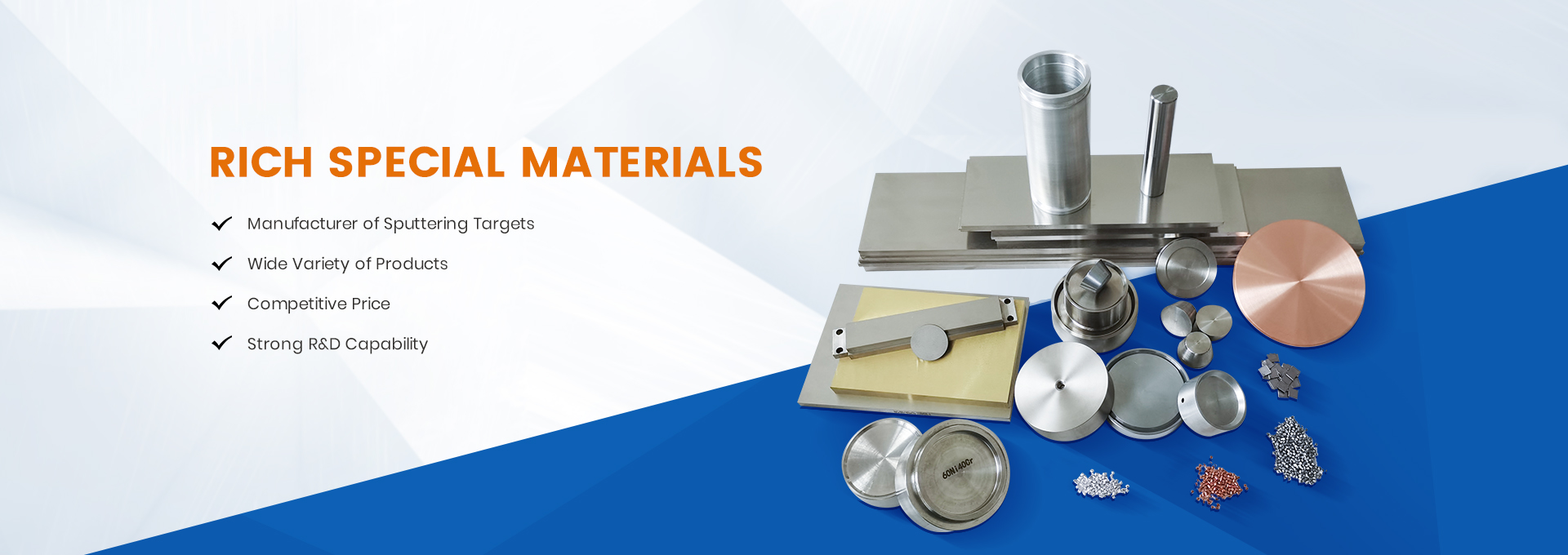


Sputtering targets are key materials in Physical Vapor Deposition (PVD) technology, widely used in semiconductors, display panels, optical coatings, hard coatings, and other fields. Their process principle is based on the bombardment of the target surface by high-energy particles, causing atoms or molecules to dislodge and deposit onto a substrate to form a thin film. This article details the process principles, key influencing factors, and typical applications of sputtering targets.
1. Basic Process Principles of Sputtering Targets
Sputter deposition is a PVD technology whose core process involves plasma generation, ion bombardment of the target, atomic sputtering, and thin-film deposition. The specific steps are as follows:
1.1 Vacuum Environment Setup
The sputtering process requires a vacuum environment to minimize gas molecule contamination of the film. Typically, the reaction chamber is first evacuated to a base vacuum , followed by the introduction of a working gas (e.g., argon, Ar), with pressure maintained in the range of 0.1~10 Pa.
1.2 Plasma Generation
A high-voltage electric field (DC, RF, or pulsed power) is applied between the target (cathode) and the substrate (anode), ionizing the argon gas to form a plasma (Ar⁺ ions and free electrons). In Magnetron Sputtering, a magnetic field (permanent magnets or electromagnetic coils) is applied behind the target to confine electron motion in a spiral trajectory, improving ionization efficiency, reducing process pressure , and increasing deposition rates.
1.3 Target Sputtering
High-energy Ar⁺ ions, accelerated by the electric field, bombard the target surface. When the ion energy exceeds the binding energy of the target atoms (sputtering threshold, typically tens to hundreds of eV), target atoms are ejected—a phenomenon called sputtering. The sputtering yield (number of atoms ejected per incident ion) depends on the target material, ion energy, and angle of incidence.
1.4 Thin-Film Deposition
The sputtered target atoms travel through the vacuum and deposit onto the substrate surface, forming a thin film. Due to the high kinetic energy of sputtered atoms , the films typically exhibit high density and strong adhesion. By adjusting substrate temperature, applying bias voltage, or introducing reactive gases (e.g., O₂, N₂), the microstructure and chemical composition of the film can be further optimized.
2. Key Process Parameters and Their Effects:
The quality and performance of sputter-deposited films are influenced by several process parameters, including:
| Parameter | Effect |
|---|---|
| Sputtering Power | Higher power → higher sputtering rate, but excessive power may cause target overheating or particle ejection. |
| Working Pressure | Higher pressure → higher plasma density, but shorter mean free path → reduced film density. |
| Target-Substrate Distance | Greater distance → improved film uniformity, but lower deposition rate. |
| Substrate Temperature | Higher temperature → enhanced atomic mobility → promotes crystallization (e.g., poly-Si deposition at high temperatures). |
| Magnetic Field Strength | Stronger field → better electron confinement → higher ionization efficiency (critical for magnetron sputtering). |
| Reactive Gas Ratio | Introduction of O₂ or N₂ enables deposition of oxide (TiO₂) or nitride (TiN) films. |
3. Classification of Typical Sputtering Processes:
Based on power supply type and process characteristics, sputter deposition can be categorized into the following major methods:
3.1 DC Sputtering
Suitable for conductive targets (e.g., Cu, Al).
Simple and cost-effective but incompatible with insulating materials.
3.2 RF Sputtering
Uses high-frequency (13.56 MHz) power to sputter insulating targets (e.g., Al₂O₃, SiO₂).
Ideal for dielectric coatings but requires higher equipment costs.
3.3 Magnetron Sputtering
Employs magnetic fields to confine electrons, improving deposition rates and energy efficiency (industry standard).
Enables large-area uniform coatings (e.g., photovoltaic glass, display panels).
3.4 Reactive Sputtering
Introduces reactive gases (e.g., O₂, N₂) during sputtering to form compound films (e.g., TiO₂, TiN).
Widely used for optical coatings and hard coatings.
4. Applications of Sputtering Targets:
Due to their precision, strong adhesion, and excellent compositional control, sputter deposition technologies are extensively applied across industries:
4.1 Semiconductor Manufacturing Copper (Cu) and Aluminum (Al) targets: Metal interconnect layers in integrated circuits. Titanium (Ti) and Tantalum (Ta) targets: Diffusion barrier layers (e.g., TaN).
4.2 Display Panels ITO (Indium Tin Oxide) targets: Transparent conductive films (touchscreens, OLEDs). Molybdenum (Mo) and Aluminum (Al) targets: Metal electrodes in TFT-LCDs.
4.3 Optical Coatings SiO₂ and TiO₂ targets: Anti-reflective and reflective coatings (e.g., camera lenses). Silver (Ag) and Gold (Au) targets: Infrared-reflective coatings (energy-efficient glass).
4.4 Hard Coatings TiN and CrN targets: Wear-resistant coatings for cutting tools and molds. DLC (Diamond-Like Carbon) targets: High-hardness, low-friction coatings.
The process principles of sputtering targets rely on high-energy particle bombardment to eject and deposit atoms into thin films. By adjusting parameters such as sputtering power, pressure, and target-substrate distance, film thickness, composition, and performance can be precisely controlled. Magnetron sputtering and reactive sputtering are the current industry standards, with broad applications in semiconductors, displays, optics, and hard coatings. Future advancements in target materials (e.g., high-entropy alloys, 2D materials) will further expand the role of sputter deposition technologies.
Post time: Oct-10-2025