



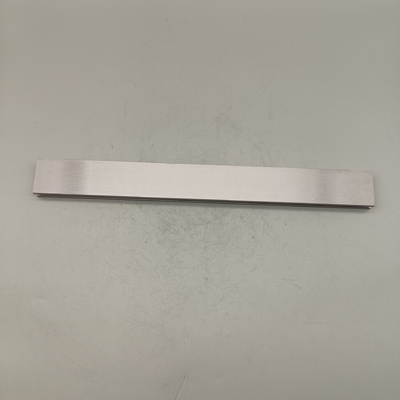
In modern semiconductor manufacturing, Physical Vapor Deposition (PVD) is a key technique for fabricating thin-film structures inside chips. At the heart of this process lies the tantalum sputtering target—one of the most essential consumables. Though it appears to be nothing more than a silver-gray metal plate, it is in fact a precision-engineered “source of atomic emission”: when bombarded by high-energy ions in a vacuum chamber, atoms are ejected from its surface and deposited onto a wafer, forming a nanoscale film with precisely controlled thickness. This film plays an irreplaceable role in copper interconnect technology: it serves as a diffusion barrier layer between the copper conductors and the silicon substrate, preventing copper atoms from migrating into the silicon and thereby ensuring the stability and reliability of the chip.
I. Basic Physical Properties of Tantalum
Tantalum (chemical symbol Ta) is a transition metal with a distinctive silver-gray luster. Its physical properties make it an ideal material for sputtering targets.
First, tantalum is a high-density metal, with a density of approximately 16.6–16.69 g/cm³ at 20°C. This high density means that tantalum atoms are packed more closely per unit volume, which facilitates the deposition of dense, high-quality thin films during the sputtering process.
Second, tantalum has an extremely high melting point of 2996°C–3017°C, with a boiling point exceeding 5400°C. This characteristic ensures that tantalum remains structurally stable under the high-temperature conditions encountered during sputtering, without softening, deforming, or undergoing abnormal grain growth—thereby guaranteeing the consistency and repeatability of film deposition.
In addition, tantalum possesses excellent ductility, allowing it to undergo significant plastic deformation without fracturing—a property that facilitates subsequent processing steps such as rolling and forging. In terms of chemical stability, tantalum is highly inert: at room temperature, it does not react with hydrochloric acid, concentrated nitric acid, or even aqua regia, and can only be dissolved by hydrofluoric acid or hot alkaline solutions. This outstanding corrosion resistance stems from a dense oxide film of tantalum pentoxide (Ta₂O₅) that forms naturally on its surface. This oxide layer not only protects the tantalum substrate but also contributes beneficially to interfacial adhesion with deposited films.
II. Key Technical Specifications of Tantalum Targets
A qualified semiconductor-grade tantalum target is defined by far more than the simple description “pure tantalum metal.” At the microscale, three dimensions form the core framework for evaluating target quality.
1. Purity
Purity is the most fundamental threshold specification for tantalum targets. The semiconductor industry imposes extremely stringent purity requirements, typically demanding 99.99% (4N) or higher, with advanced process nodes (such as 14nm and below) often requiring 99.999% (5N) or even 99.9995% (5N5) purity levels. The significance of ultra-high purity lies in the fact that even trace impurities—whether radioactive elements (such as uranium and thorium), alkali metals (such as sodium and potassium), or transition metals—can act as defect centers in nanoscale thin films, leading to current leakage, threshold voltage drift, increased contact resistance, or even premature device failure. Therefore, every step from tantalum powder purification to final target forming must be carried out under highly controlled conditions.
2. Grain Size
The interior of a tantalum target consists of countless microscopic crystalline grains. The size of these grains and their uniformity of distribution directly affect the stability of the sputtering process. Advanced process nodes require the average grain size to be controlled below 60 micrometers (μm), with the variation across different positions on the same target kept as small as possible—typically requiring a range of less than 15 μm. Non-uniform grain size can cause differences in atomic emission rates across the target surface during sputtering, which in turn results in poor thickness uniformity of the deposited film across the wafer, directly impacting chip yield.
3. Crystallographic Texture
“Texture” is the most subtle and difficult technical parameter to control in target fabrication. It describes the preferred crystallographic orientation of grains in space. Different crystal planes—such as {100}, {110}, and {111}—exhibit different sputtering yields; atoms on certain orientations are more readily ejected from the target surface. An ideal tantalum target requires a uniform distribution of the three main texture components, avoiding excessive dominance of any single orientation (particularly {111}). The essence of texture control lies in precisely regulating the recrystallization behavior and grain growth direction during rolling and heat treatment—a task that demands extremely refined matching of processing parameters including deformation amount, deformation direction, annealing temperature, and holding time.
III. Manufacturing Methods for Tantalum Targets
The production of tantalum targets constitutes a complete process chain—from high-purity tantalum powder to precision-formed components—with the core objective of achieving the three specifications described above through coordinated control across all process steps.
Step 1: Preparation of High-Purity Tantalum Powder. The most widely adopted industrial route uses potassium fluorotantalate (K₂TaF₇) as the raw material, which is reduced by metallic sodium via a thermal reduction reaction to produce high-purity tantalum powder. This method offers the advantages of mature technology, high production capacity, and relatively high initial purity.
Step 2: Compaction and Sintering. The high-purity tantalum powder is loaded into an elastic mold and compacted under pressures of several hundred megapascals using cold isostatic pressing (CIP) to obtain a uniformly dense green compact. This compact is then placed in a vacuum sintering furnace and sintered at high temperatures of approximately 2600°C–3000°C, transforming the mechanical bonding between powder particles into robust metallic bonds while further densifying the material. A distinctive advantage of the powder metallurgy route is that the initial grains are fine and the compaction conditions are consistent across all positions, yielding a tantalum blank with far superior microstructural uniformity compared to conventional cast ingots.
Step 3: Thermomechanical Processing—Rolling and Annealing. This is the most critical technical stage in target fabrication. The sintered tantalum blank is progressively reduced to the target thickness through multiple passes of rotary rolling (such as cross rolling or circumferential rolling). During this process, coarse grains are broken down and grain orientations are redistributed. Interspersed at different stages are precisely controlled recrystallization annealing treatments, which allow the fragmented grains to nucleate anew and grow to the desired size under appropriate conditions, while simultaneously homogenizing the texture distribution. The design of rolling passes, the allocation of deformation amounts, and the combination of annealing temperature and time collectively determine the final grain size and texture characteristics of the target.
An alternative route, ingot metallurgy, is also used for some high-end applications: a high-purity tantalum ingot is first produced via electron beam melting, followed by forging, rolling, and heat treatment. This method offers the advantage of producing larger-sized targets, though it presents greater challenges in impurity control and texture uniformity.
IV. Major Application Areas
1. Semiconductor Chip Manufacturing (Core Application)
The most critical and irreplaceable application of tantalum targets lies in copper interconnect technology for semiconductor integrated circuit fabrication. In advanced logic and memory chips, the tantalum (Ta) and tantalum nitride (TaN) thin films deposited from tantalum targets constitute the bilayer diffusion barrier between the copper conductors and the silicon substrate. This barrier must simultaneously fulfill three functions: effectively blocking copper diffusion into silicon, providing good interfacial adhesion with both the copper layer and the dielectric layer, and maintaining low contact resistance. From the 90nm node down to the most advanced processes, tantalum-based barriers have remained the standard solution for copper interconnect technology.
2. Optical Coatings
Leveraging tantalum’s high refractive index and excellent optical stability, tantalum targets are used to produce various precision optical thin films, including anti-reflective coatings, reflective coatings, and beam-splitting coatings for camera lenses, projectors, microscopes, and other optical systems.
3. Hard Coatings and Surface Hardening
Through reactive sputtering to deposit hard compound films such as tantalum nitride (TaN), tantalum targets can be used for surface hardening of cutting tools, molds, and mechanical components, significantly improving their wear resistance and corrosion resistance, thereby extending service life.
4. Electronic Components
In high-end capacitor manufacturing, tantalum targets can serve as anode thin-film materials, leveraging the high dielectric constant of tantalum oxide to enhance device performance.
Conclusion
In essence, a tantalum sputtering target is the product of seamlessly integrating tantalum’s inherent physical and chemical attributes—high density, high melting point, excellent ductility, and chemical stability—with precisely engineered microscale features including ultra-high purity, uniform grain size, and ideal crystallographic texture. It embodies the ultimate pursuit of microstructural control in materials science while supporting the semiconductor industry’s exacting demands for nanoscale thin-film performance. To the naked eye, it appears as nothing more than a silver-gray metal plate; but in the microscopic realm, every precise adjustment of grain orientation and every carefully controlled heat treatment ultimately manifest in the yield and performance of the chips it helps create.
Post time: Jul-24-2026