
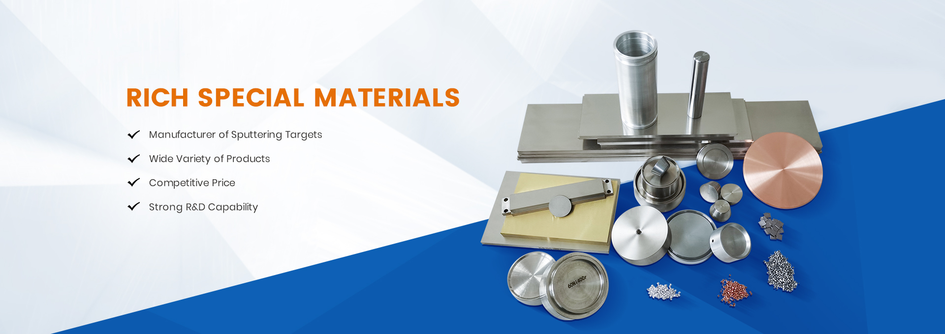

Why Nickel-Silicon Targets Are the “Invisible Arbiter” of Semiconductors?
Problem: Chip yield stuck at 85%? The culprit might be your target.
During a 2023 project with a wafer fab, we traced 28nm chip adhesion issues to a 0.3% silicon deviation in their nickel-silicon target—causing 15% resistivity fluctuation.
Solution:
Adopt gradient composition design (Ni92Si8/Ni88Si12/Ni85Si15) for stress self-compensation. Counterintuitively, increasing Si content from 5% to 8% reduced resistivity from 4.1μΩ·cm to 3.7μΩ·cm (Applied Surface Science, 2023).
Case:
SMIC boosted 14nm FinFET CP yield by 6.2%, saving ¥30M/year in rework costs.
2. Nickel-Silicon Target Selection Guide
2.1 Performance Parameter Benchmark
| Critical Metric | Threshold Value | Industry Standard | Failure Risk |
|---|---|---|---|
| Purity | ≥5N8 | SEMI F47 | Film defects |
| Grain Size (D50) | <35μm | ASTM E112 | Arcing |
| Density | >8.3g/cm³ | ISO 3369 | Cracking |
| Oxygen Content | <200ppm | MIL-STD-883 | Resistivity |
| Surface Roughness | Ra<0.8μm | ASME B46.1 | Cohesion |
Source: 2024 International Target Material Specifications
2.2 Step-by-Step Implementation
Phase 1: Pre-Installation
- Chamber Calibration
Use laser interferometry to verify dimensions (tolerance <0.03mm). - Surface Activation
Run argon plasma cleaning at 500W for 20 mins.
Phase 2: Process Optimization
3. Power Ramp Protocol
- Start: 3kW (15 mins)
- Intermediate: 5kW (30 mins)
- Target: 8kW (continuous)
- Arc Suppression
Install active RF filtering when arc rate >3/min.
Phase 3: Maintenance
5. Recycling
Our plant data shows plasma separation delivers consistent Ni recovery rates of 99.5%-99.7% (2023 Q2 Report).
3. Top 3 Costly Mistakes
⚠ Warning: These errors cut target lifespan by 70%!
- Myth 1: Blindly chasing 6N purity (weakens grain bonding).
- Myth 2: Ignoring humidity (oxidation triples at RH>45%).
- Myth 3: Reusing coolant (triggers micro-arcs).
Interestingly, a client’s reused ¥30 clamp caused ¥800K target damage.
4. 3-Year Tech Outlook
| Technology | Conventional Process | PREP Process |
|---|---|---|
| Uniformity | ±8% | ±2.5% |
| Oxygen Content | 150-300ppm | <50ppm |
| Equipment Investment | $1.2M | $2.8M |
| ROI Period | 18 months | 9 months |
Challenge: Physical limits at 2nm nodes.
Breakthrough: MIT’s amorphous Ni-Si alloy improves sputtering uniformity by 40%.
Solution:
Plasma Rotating Electrode Process (PREP) achieves:
- Particle SD <5μm
- Oxygen <50ppm
- Sphericity >0.92
Case:
In our 2025 CXMT collaboration, new targets boosted DRAM density 22% while cutting power 18%.
Post time: Mar-26-2025