


How to Choose the Right Cobalt Sputtering Target? A Complete Guide from Beginner to Expert
In the semiconductor manufacturing field, one material is quietly reshaping the landscape of advanced processes—cobalt sputtering targets. It serves as the “invisible hero” in interconnect layers for sub-7nm chips and stands as the core material for MRAM memory devices. However, choosing the wrong cobalt target can lead to the scrapping of an entire furnace of wafers. How can you ensure you select and use the right one? This article will guide you through the complete process of selecting and utilizing cobalt sputtering targets, from the ground up.
1. What is a Cobalt Sputtering Target and Why is it So Important?
A cobalt sputtering target is a critical consumable in the physical vapor deposition process. Simply put, it’s a piece of high-purity metallic cobalt. Inside a vacuum chamber, it’s bombarded by high-energy particles, causing cobalt atoms to be “sputtered” off and deposited onto a wafer or glass substrate, forming a functional thin film only tens of nanometers thick.
Counterintuitively, although cobalt is more expensive than copper, it has replaced copper in some interconnect applications for sub-7nm advanced processes. Why? Because cobalt’s electromigration resistance is far superior to copper’s, and it fills small trenches more uniformly. The quality of a cobalt sputtering target directly determines chip yield and reliability.
Interestingly, according to data from QYResearch, the global market for high-purity cobalt sputtering targets was approximately $32.48 million in 2024 and is projected to reach $56.02 million by 2031, with a compound annual growth rate of 8.2%. This growth is driven by the explosive demand for AI computing power and advanced packaging technologies.
2. How to Choose the Right Cobalt Sputtering Target?
Selection isn’t just guesswork. During a 2025 project assisting a memory chip fab with target replacement, our team discovered that a seemingly minor composition deviation led to a 30% drop in the tunneling magnetoresistance ratio of MRAM devices. The selection framework below will help you avoid such pitfalls.
2.1 Step 1: Define the Purity Level
Purity is the lifeline of a cobalt sputtering target. Purity requirements vary significantly across different applications:
| Application Field | Recommended Purity | Key Impurity Control |
|---|---|---|
| MRAM/STT-MRAM | ≥99.95% (3N5) | Fe, Ni, Cu, O, S ≤ ppm level |
| Advanced Logic Chips (sub-7nm) | ≥99.999% (5N) up to 7N | Control down to ppb level |
| Hard Drive Magnetic Recording Layer | ≥99.95% (3N5) | Focus on magnetic consistency |
| Research / General Coating | 99.9% – 99.99% | Determine based on experimental needs |
⚠ Note: Don’t blindly pursue the highest purity. A 5N-grade cobalt target can cost several times more than a 4N-grade one. If your application doesn’t require it, it’s a waste of resources. However, for semiconductor front-end processes, always choose verified high-purity products.
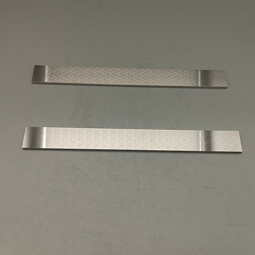
2.2 Step 2: Confirm Target Shape and Dimensions
Cobalt targets mainly come in two shapes: circular and rectangular. Your choice depends on your sputtering equipment:
- Circular targets: Common diameters include 1 inch, 2 inches, 3 inches, 4 inches, with thickness typically between 1-5mm.
- Rectangular targets: Customized based on the equipment chamber size.
One easily overlooked detail is the thickness limitation for magnetic targets. Since cobalt is a ferromagnetic material, most of the magnetic flux lines will pass through the target interior, weakening the magnetic field on the target surface. Therefore, the thickness of a cobalt target is usually recommended to be no more than 3mm; some equipment requires control within 2mm; otherwise, it may be difficult to initiate and sustain plasma.
2.3 Step 3: Select the Manufacturing Process
There are two primary manufacturing routes for high-purity cobalt targets:
- Melting and Casting: Suitable for pure cobalt and most cobalt alloys (like CoFe, CoNi). Through vacuum induction melting followed by directional casting, a columnar grain structure can be achieved, enhancing magnetic pass-through flux.
- Powder Metallurgy: Suitable for refractory or brittle materials (like high-boron CoFeB). Through vacuum hot pressing and sintering, a fine, uniform grain structure is obtained, with density close to the theoretical value.
For instance, if you need a CoFeB target for the magnetic tunnel junction in MRAM, the powder metallurgy route is often the better choice because it allows precise control over boron distribution, preventing composition segregation.
2.4 Step 4: Evaluate the Bonding Process
Most cobalt targets require bonding to a copper backing plate. Why? Because cobalt has poor thermal conductivity, while the copper backing plate effectively dissipates heat, preventing the target from deforming or cracking due to high temperatures during sputtering.
When inspecting bonding quality, focus on two key indicators:
- Bonding rate: Should be ≥95%
- Thermal resistance: The lower, the better
3. Typical Application Scenarios for Cobalt Targets
Understanding application scenarios helps you select a cobalt target more precisely. Here are several mainstream directions:
3.1 Advanced Semiconductor Interconnects
In logic chips at 7nm and below, cobalt targets are used to deposit barrier layers and contact fill layers for copper interconnects. While cobalt’s resistivity is higher than copper’s, its electromigration lifetime at small dimensions far exceeds that of copper.
3.2 Magnetic Random Access Memory
MRAM and STT-MRAM represent the future direction of memory technology. Their core structure is the magnetic tunnel junction, composed of a CoFeB magnetic layer, an MgO tunnel layer, and another CoFeB layer. Here, the cobalt target is not pure cobalt but an alloy target with a specific composition ratio.
3.3 Hard Disk Magnetic Recording Media
The magnetic recording layer in traditional hard drives consists of cobalt-based alloys like CoCrPt. This application demands extremely high magnetic consistency from the target.
4. Common Misconceptions and Operational Guidelines
⚠ Common Misconceptions Warning
| Misconception | Reality |
|---|---|
| “Higher purity is always better” | High purity comes with high cost; choose reasonably based on application needs. |
| “All cobalt targets are the same” | Manufacturing processes (melting vs. powder) and bonding processes differ significantly. |
| “Any thickness is fine for magnetic targets” | Cobalt target thickness is limited; exceeding limits may prevent plasma ignition. |
| “Any supplier is fine” | High-end targets rely on accumulated process expertise; choose vendors with proven certification. |
Practical Guide: 5 Steps to Master Cobalt Target Usage
Step 1: Inspection Before Unpacking
Check for packaging integrity. High-purity cobalt targets are usually vacuum-sealed. If the package is damaged, reassess the potential for surface oxidation.
Step 2: Cleaning Before Installation
Unpack in a cleanroom environment, wearing powder-free gloves. Gently wipe the target surface with anhydrous ethanol and a lint-free cloth to remove particles absorbed during transport.
Step 3: Equipment Parameter Setup
Due to cobalt’s magnetic properties, the sputtering voltage is typically higher than for non-magnetic targets. Start with a lower initial power and ramp up gradually to avoid plasma instability.
Step 4: Pre-Sputtering
After installing a new target, perform pre-sputtering (about 10-30 minutes) to remove surface oxides and contaminants, stabilizing the sputtering rate.
Step 5: Process Monitoring
Record parameters such as target lifespan, sputtering power, voltage, chamber pressure, etc. Consider replacing the target when the sputtering rate drops by more than 15%.
With the continued surge in demand for AI chips, HBM high-bandwidth memory, and advanced packaging technologies, the demand for cobalt targets will maintain high growth. Simultaneously, the wave of domestic substitution is reshaping the supply chain landscape. Whether you’re in semiconductor manufacturing or a research institution, mastering the selection and usage techniques for cobalt targets is a crucial step toward advancing high-end manufacturing.
Cobalt Target Selection Practical Checklist
- Application Confirmation: Is it for semiconductors, MRAM, hard drives, or research?
- Purity Matching: 4N, 5N, or higher? Does it meet process requirements?
- Dimensions & Specs: Does the diameter/width, length, thickness meet equipment requirements? For magnetic targets, is the thickness ≤3mm?
- Bonding Check: Is it bonded to a copper backing plate? Is the bonding rate ≥95%?
- Process Route: Melting or powder metallurgy? Is it suitable for your material system?
- Supplier Qualifications: Does the supplier have a proven track record with wafer fabs? Can they provide traceability documentation?
- Budget Evaluation: Does it include bonding and shipping costs? Does the lead time match project milestones?
- Pre-Sputtering Plan: Is sufficient pre-sputtering time reserved?
Post time: Mar-24-2026