
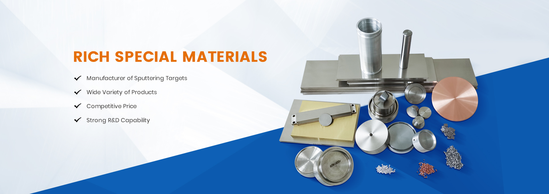




As a critical consumable in physical vapor deposition (PVD) processes, the quality of molybdenum sputtering targets directly determines the performance and yield of thin-film devices. With flat panel displays evolving toward larger sizes and higher resolutions, and semiconductor processes becoming increasingly precise, the market has set extremely stringent requirements for target purity, density, and grain size uniformity.
As a professional supplier of high-performance refractory metal materials, we are committed to providing full-generation, high-quality molybdenum and molybdenum alloy sputtering targets. Our solutions empower global manufacturing customers to overcome technical bottlenecks and achieve efficient, stable mass production.
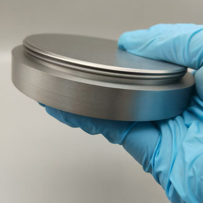
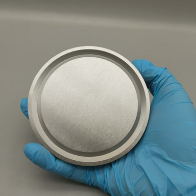
Why Choose Our Molybdenum Sputtering Targets?
1. High Purity for Superior Thin-Film Performance
Purity is the foremost indicator of sputtering target quality. Impurities in the material are the primary source of thin-film contamination, often leading to particle defects and reduced pixel performance. Our pure molybdenum targets achieve a purity level of no less than 99.97%, This ensures high-purity sputtered films with excellent electrical properties from the very source.
2. High Density for Significantly Enhanced Sputtering Efficiency
Porosity within low-density targets can release trapped gases under bombardment, causing large-particle splashing that severely compromises film quality. Through advanced large-scale rolling deformation and specialized sintering processes.
3. Fine and Uniform Grain Structure for Consistent Coating Uniformity
Grain size and distribution have a major impact on sputtering rate and film thickness uniformity. Fine grains with narrow size distribution not only enable faster sputtering but also produce more uniform film thickness across the substrate. Using advanced plastic deformation and heat treatment technologies, we consistently control grain size , ensuring long-term sputtering stability and repeatability.
roduct Specifications and Applications
Product Forms and Materials
We offer a wide range of configurations including square targets, strip targets, and rotary targets, . In addition to pure molybdenum (Mo) targets, we also provide molybdenum alloy targets doped with elements such as Nb, Ni, and Ti. These alloy-based films deliver superior corrosion resistance and adhesion, making them an increasingly preferred choice in high-end display applications.
Key Application Areas
- Flat Panel Displays (FPD): As electrode and wiring materials in TFT-LCD and OLED panels, molybdenum targets offer high melting points, low resistivity, and excellent corrosion resistance—significantly enhancing display brightness, contrast, and service life.
- Semiconductor Chips: In integrated circuit manufacturing, molybdenum and molybdenum alloy targets are widely used as barrier layer materials, effectively preventing copper diffusion and ensuring high chip reliability.
- Thin-Film Solar Cells: Ideal for back-contact electrode preparation in CIGS (copper-indium-gallium-selenide) and other thin-film photovoltaic technologies.
Conclusion
From G3 to G10.5, from display panels to the frontiers of semiconductor technology, our molybdenum sputtering targets have earned the trust of global high-end manufacturing customers through their core advantages of high purity, high density, and fine uniform grain structure. If you are seeking a stable, high-performance sputtering solution, we invite you to contact us for more technical data or custom-engineered proposals.
Post time: Jul-31-2026