
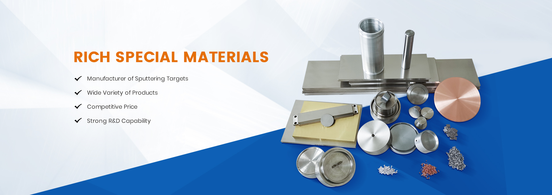


Ceramic targets are key materials in thin film deposition techniques such as physical vapor deposition (PVD) and chemical vapor deposition (CVD). They are widely used in semiconductors, optoelectronics, energy, and protective coatings due to their high melting points, superior hardness, excellent chemical stability, and tunable electrical/optical properties.
Ceramic targets can be categorized based on composition and functionality:
1. Oxide Ceramic Targets
Transparent Conductive Oxides (TCOs):
AZO (Al-doped ZnO): A low-cost alternative to ITO, used in solar cells and touch panels.
ITO (In₂O₃:SnO₂): High conductivity and transparency, ideal for display panels.
FTO (F-doped SnO₂): Heat-resistant, applied in photovoltaic glass.
Dielectric Oxides:
Al₂O₃: High insulation for gate dielectric layers.
SiO₂: Optical coatings and passivation layers.
TiO₂: Photocatalytic and self-cleaning coatings.
2. Nitride Ceramic Targets
TiN, CrN: Ultra-hard wear-resistant coatings for cutting tools and molds.
AlN: High thermal conductivity for LED heat dissipation substrates.
Si₃N₄: High-temperature structural materials for bearings and engine components.
2.Carbide Ceramic Targets
SiC: High-temperature and corrosion resistance for semiconductor power devices.
WC: Ultra-hard material for cutting tools.
TiC: Hard coatings for aerospace components.
4. Chalcogenide Targets
CdTe, CIGS: Thin-film solar cell absorbers.
ZS, ZnSe: Infrared optical window materials.
What is the Fabrication Methods for Ceramic Targets?
3.1 Powder Synthesis
Solid-State Reaction: Oxide mixtures calcined (e.g., ZnO + Al₂O₃ → AZO).
Sol-Gel Method: Hydrolysis and polycondensation of precursors to form nanopowders.
Co-Precipitation: Metal salt solutions co-precipitated and calcined for uniform powders.
3.2 Forming and Sintering
Cold Isostatic Pressing (CIP): High-pressure compaction for high-density green bodies.
Hot Pressing (HP): High temperature + pressure to minimize porosity.
Spark Plasma Sintering (SPS): Rapid sintering to suppress grain growth.
Hot Isostatic Pressing (HIP): High temperature and pressure to eliminate defects.
3.3 Post-Processing
Machining: Precision grinding to required dimensions .
Bonding: backing plates for thermal conduction to prevent cracking.
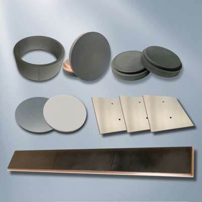
4. Applications of Ceramic Targets
|
Application |
Typical Targets |
Function |
| Display Panels | ITO, AZO | Transparent conductive electrodes (TFT-LCD, OLED) |
| Photovoltaics | CdTe, CIGS | Absorber/window layers |
| Semiconductor Devices | Al₂O₃, HfO₂ | High-k gate dielectrics |
| Hard Coatings | TiN, CrN, WC | Wear-resistant layers for tools |
| Optical Coatings | SiO₂, TiO₂ | Anti-reflective/mirror coatings |
| Biomedical | ZrO₂, HA (Hydroxyapatite) | Artificial bones/dental implants |
Ceramic targets, as the core materials for modern functional thin film fabrication, play an indispensable role in semiconductors, optoelectronics, energy, and hard coatings due to their excellent electrical, optical, and mechanical properties. From conventional oxides (e.g., ITO, AZO) to advanced nitrides (e.g., TiN, AlN) and emerging chalcogenides (e.g., CIGS), various ceramic targets continue to push performance boundaries through precise composition design and advanced fabrication techniques (e.g., SPS sintering, nanocomposite technology). Despite challenges such as high costs and large-scale uniformity, the future development of ceramic targets will focus on cost reduction, nanostructuring, and environmental sustainability to meet the demands of flexible electronics and green energy, thereby serving as a critical material foundation for next-generation devices.
Post time: Sep-01-2025