
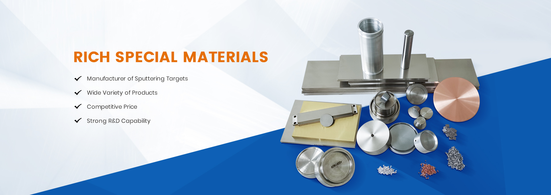


In magnetron sputtering technology, indium bonding is the most commonly used thermal management process for joining sputtering targets (especially brittle materials like ITO ceramics or silicon) to a copper backplate. The indium layer acts as both a “thermal conductive bridge” and a “mechanical adaptation layer.”
However, during actual sputtering operations, a troublesome problem often arises: After several hours or cycles of sputtering within the vacuum chamber, the indium layer peels away from the target (or the backplate), leading to localized overheating, arcing, or even cracking of the target.
This article analyzes the underlying causes of indium layer detachment during active sputtering from the perspectives of thermodynamics, interfacial science, and mechanical stress.
1. Heat Accumulation and the “Softening Threshold” of Indium
The physical properties of indium define its “fragile boundaries”:
- Melting Point: 156.7℃
- Recrystallization Temperature: Occurs at room temperature
- Softening Point: The yield strength of indium drops sharply around 100℃ ~ 120℃.
Thermal Balance Failure During Sputtering:
During sputtering, the target surface is bombarded by ions, with approximately 75%-90% of the energy converting into heat.
- Heat Conduction Path: Heat must pass through three interfaces—”Target-Indium-Copper Backplate”—before being finally carried away by cooling water behind the backplate.
- Failure Trigger Point: If the sputtering power is too high or the cooling water flow is insufficient, the temperature of the indium layer rises rapidly. Once it exceeds 100℃, the indium begins to soften, and its shear resistance decreases significantly.
- Consequence: The softened indium layer cannot effectively constrain the displacement of the target caused by thermal expansion. This creates localized gaps, further worsening heat conduction and leading to a “thermal runaway” situation. Eventually, the indium layer undergoes plastic flow (being squeezed out) or the adhesive interface tears.
2. The “Mismatch Battle” of Thermal Expansion Coefficients
This is the core physical driving force behind indium layer detachment. The coefficients of thermal expansion (CTE) of the three materials differ significantly:
- Copper Backplate: Approx. 16.8 × 10⁻⁶ /K
- Indium Layer: Approx. 32.1 × 10⁻⁶ /K (very soft, easily deformed)
- Common Target Material (e.g., ITO Ceramic): Approx. 8.5 × 10⁻⁶ /K
Stress Evolution During Sputtering Heating:
- Heating Phase: Both the target (small expansion) and the copper backplate (large expansion) expand, but at different rates. The copper backplate tries to “stretch open” more, while the target relatively “resists.”
- Generation of Shear Stress: This expansion differential generates significant shear stress at the indium interface. Due to indium’s good ductility, it initially absorbs this stress through plastic deformation.
- Fatigue and Peeling: During repeated cycles of heating (sputtering) and cooling (downtime/standby), the indium layer is subjected to alternating stress. When the stress exceeds the bonding strength between the indium and the target’s backside, micro-cracks begin to initiate at the interface. Crack propagation eventually leads to large-area detachment.
3. “Inherent Deficiencies” in Interfacial Bonding Strength
If hidden defects exist in the pre-sputtering bonding process, they will be dramatically amplified under the high-temperature, high-vacuum conditions of sputtering:
- Poor Wetting (Cold Solder Joints):
- If the backside of the target is heavily oxidized, or if cleaning is inadequate (oil residue, dust), molten indium cannot form a continuous intermetallic bond with the target surface; it merely “sits” on top of it.
- Manifestation During Sputtering: Upon heating, areas with voids (due to poor wetting) exhibit extremely high thermal resistance. Local temperatures spike instantly, causing the surrounding indium to melt, contract, and enlarge the voids, ultimately leading to detachment.
- Residual Stress:
- If the cooling rate is too fast during the bonding process, significant residual stress can remain locked inside the indium layer.
- Manifestation During Sputtering: The externally applied thermal stress superimposes onto the internal residual stress, instantly reaching the indium’s strength limit and causing “cleavage-type” detachment.
4. The “Drastic Temperature Difference” on the Cooling Side
Sputtering equipment’s water cooling system typically maintains the copper backplate around 20℃, while the target surface temperature can reach several hundred degrees. This substantial temperature gradient (△T) across the bonding layer has significant effects:
- Thermal Expansion Gradient: Indium near the target side is hot and expands greatly; indium near the copper plate side is cool and contracts. This non-uniform expansion along the thickness direction can either tear the indium layer apart from within or cause it to detach from the cooler copper plate (as the indium on the cool side contracts more severely).
5. On-Site Diagnosis of Common Detachment Modes
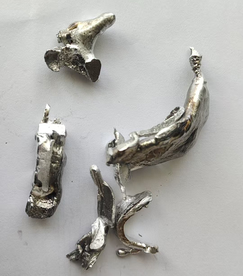
By examining the morphology of the separated surfaces, the failure cause can often be inferred:
| Detachment Phenomenon | Direct Cause | Root Cause |
|---|---|---|
| Indium remains on the copper plate; target backside is clean | Target/Indium interface failure | Target backside not properly cleaned or lacks a metallized coating (poor wetting) |
| Indium remains on the target; copper plate surface is clean | Copper plate/Indium interface failure | Copper plate surface oxidation or contamination before bonding; excessive thermal stress on the cooling side |
| Tear occurs within the indium layer itself; residue on both sides | Cohesive failure within indium layer | Indium layer too thick, thermal fatigue, or operating temperature too high causing loss of indium strength |
| Target edges lifting; signs of indium being squeezed out | Thermal overload and plastic flow | Excessive sputtering power, insufficient cooling, indium melting and being extruded |
6. Conclusion and Preventive Recommendations
Indium detachment during sputtering is essentially a failure where the ”heat input” exceeds the balance point between “interfacial bonding strength” and the “material’s temperature tolerance.”
Recommended Preventive Measures:
- Optimize Bonding Process: Ensure the target backside undergoes ultrasonic cleaning, ion bombardment, or coating with a transition layer (e.g., nickel/molybdenum) to enhance wetting.
- Control Indium Thickness: The ideal indium layer thickness is typically between 0.1mm and 0.3mm. Excessive thickness increases thermal resistance and fatigue risk.
- Ramp Power Gradually: When commissioning a new target, power should be increased slowly, allowing the entire system (especially the soft indium) to adapt gradually to the thermal stress distribution.
- Monitor Water Temperature and Flow: Ensure adequate cooling water flow and stable temperature to prevent instantaneous high temperatures caused by poor flow.
Understanding these mechanisms helps process personnel implement comprehensive control, from the “bonding workshop” to the “sputtering machine,” fundamentally solving the persistent problem of indium detachment.
Post time: Feb-24-2026